

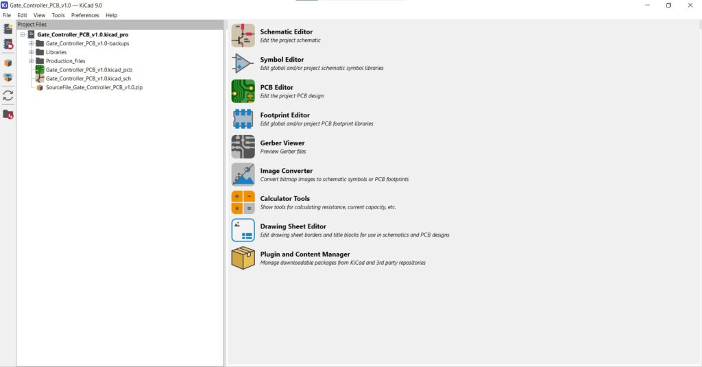
Designing a circuit board used to require expensive software and powerful computers. Today, that has changed. KiCad is one of the best free PCB design tools available, trusted by hobbyists, students, startups, and professional engineers around the world.
In this article, we’ll explore what KiCad is, why it’s so popular, and how it can help you with circuit board design software needs without spending a single dollar.
What Is KiCad?
KiCad is an open-source PCB layout software that allows you to design electronic circuits and turn them into manufacturable printed circuit boards. It supports the complete PCB design workflow, from schematic capture to final Gerber file generation.
Unlike many paid tools, KiCad does not limit board size, number of layers, or features. This makes it an excellent choice for beginners and professionals alike.
Why KiCad Is a Popular PCB Design Tool
KiCad has gained massive popularity because it combines powerful features with zero cost. Here are some key reasons engineers choose it:
- Completely free and open source
- No licensing restrictions
- Runs on Windows, macOS, and Linux
- Strong community support and regular updates
For anyone looking for free PCB design, KiCad is often the first recommendation.
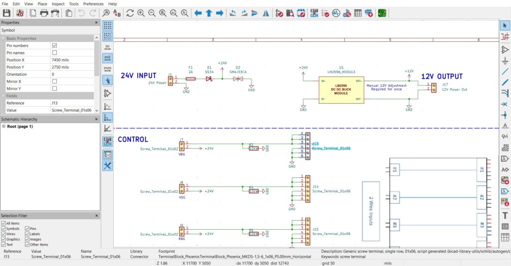
Schematic Capture Made Simple
The design process starts with schematics, and KiCad’s schematic editor is clean and easy to use. You can:
- Create professional circuit diagrams
- Use a large built-in symbol library
- Design custom symbols if needed
- Run electrical rule checks (ERC)
This step ensures your circuit is logically correct before moving to PCB layout.
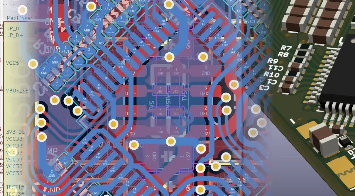
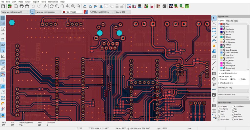
Powerful PCB Layout Software
KiCad’s PCB editor allows you to convert schematics into real circuit boards. It supports:
- Single-layer to multi-layer boards
- Manual and interactive routing
- Differential pairs and length matching
- Ground planes and copper pours
These features make KiCad suitable not only for simple projects but also for complex designs like microcontroller boards, power supplies, and RF circuits.
Libraries and 3D Viewer
One standout feature of KiCad is its 3D viewer. With just one click, you can see how your board will look in real life.
Benefits include:
- Checking component placement
- Verifying connector orientation
- Creating visuals for documentation or clients
KiCad also supports custom footprints and integrates well with manufacturer libraries, making it practical for real-world designs.
Manufacturing-Ready Output
When your design is complete, KiCad generates all required manufacturing files, including:
- Gerber files
- Drill files
- Pick-and-place data
- Bill of Materials (BOM)
These outputs work with almost all PCB manufacturers, allowing you to order boards without extra conversion steps.
KiCad support many 3rd party plugins to generate these output files, like KiCad to JLCPCB (JLCPCB is a popular PCB fabricator worldwide based in china)
This makes KiCad a reliable circuit board design software from idea to production.
Who Should Use KiCad?
KiCad is ideal for:
- Electronics students learning PCB design
- Hobbyists building DIY projects
- Startups reducing software costs
- Engineers needing a reliable backup tool
If you are searching for pcb design tools that are powerful, flexible, and free, KiCad is an excellent choice.
Final Thoughts
KiCad proves that you don’t need expensive software to design professional-quality circuit boards. With powerful features, active development, and a growing user community, it has become one of the most trusted names in free PCB design.
Whether you are designing your first PCB or your hundredth, KiCad gives you the tools to turn ideas into real hardware—without limits.