Why RS232 Refuses to Die
When you walk into any server room, industrial plant, or hardware lab, there is a clear disconnect. We live in a world of high-speed USB-C and wireless everything, but the backbone of our most critical infrastructure still uses a language that was standardized in the 1960s: RS232. Whether you are configuring a network switch or diagnosing legacy lab equipment, a robust serial cable to usb solution remains the undisputed king of reliability.
But there’s a catch. Good luck finding a native 9-pin serial port on a modern laptop. It is almost impossible.
A reliable USB to serial adapter seamlessly bridges the gap between modern, high-speed USB data packets and rugged, high-voltage serial logic.
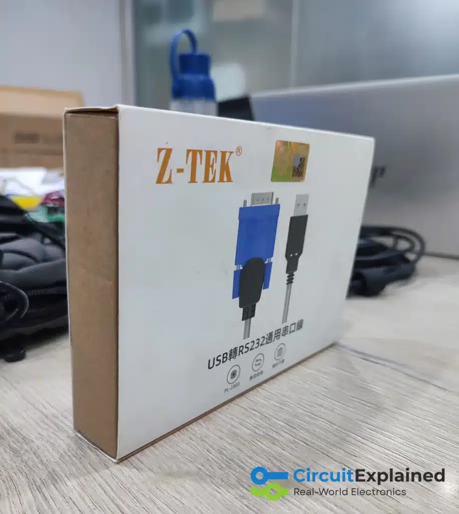
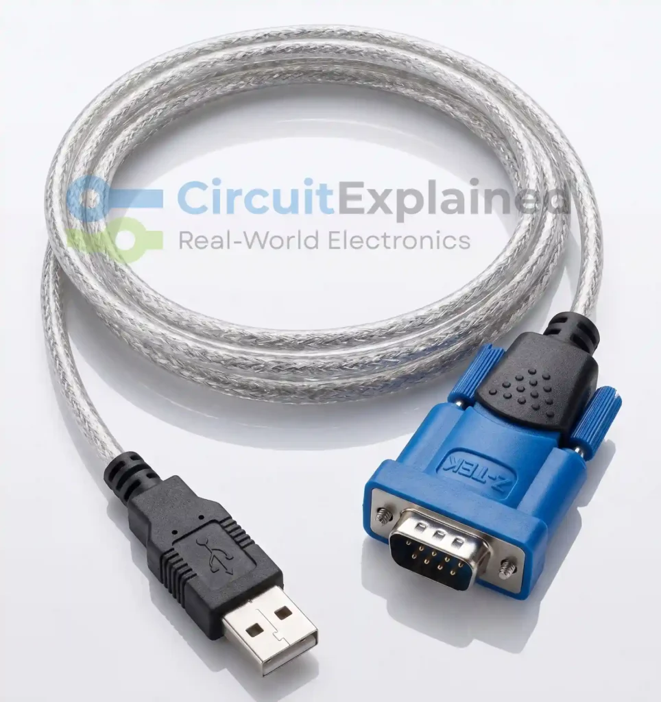
In this teardown, we are going to crack open a reliable USB 2.0 serial Adapter comes from Z-TEK with the bridge IC Prolific PL2303GT. We will look at the internal circuit and schematic to figure out exactly how this USB RS232 adapter steps a standard 5V USB supply up to the ±12V needed to drive a true serial line. Whether you are searching for an RS232 to USB converter or a generic USB adapter serial cord, the internal magic is largely the same.
The DB9 Connector and RS232 Pinout
Before we take a scalpel to the plastic housing of our USB to RS232, let’s look at the business end of the device: the 9-pin D-subminiature (DB9) male connector.
When configuring a DB9 to USB setup, it helps to understand the physical interface. While the RS232 standard originally utilized a massive 25-pin connector, the PC industry standardized on the much smaller DB9 port decades ago. Even though there are nine pins available, most basic applications only strictly require three of them to establish full-duplex (two-way) communication:
- Pin 2 – RXD (Receive Data): Listens for incoming data.
- Pin 3 – TXD (Transmit Data): Sends data out.
- Pin 5 – GND (Ground): The common voltage reference line.
The remaining pins are primarily dedicated to hardware flow control. These were originally designed for old dial-up modems to signal when they were ready to receive data or if a carrier signal was detected. While many hobbyists ignore these pins today, specialized industrial controllers still rely heavily on them. If you are using a premium USB to serial adapter, these hardware flow control lines are fully supported in the silicon to prevent data buffer overruns.
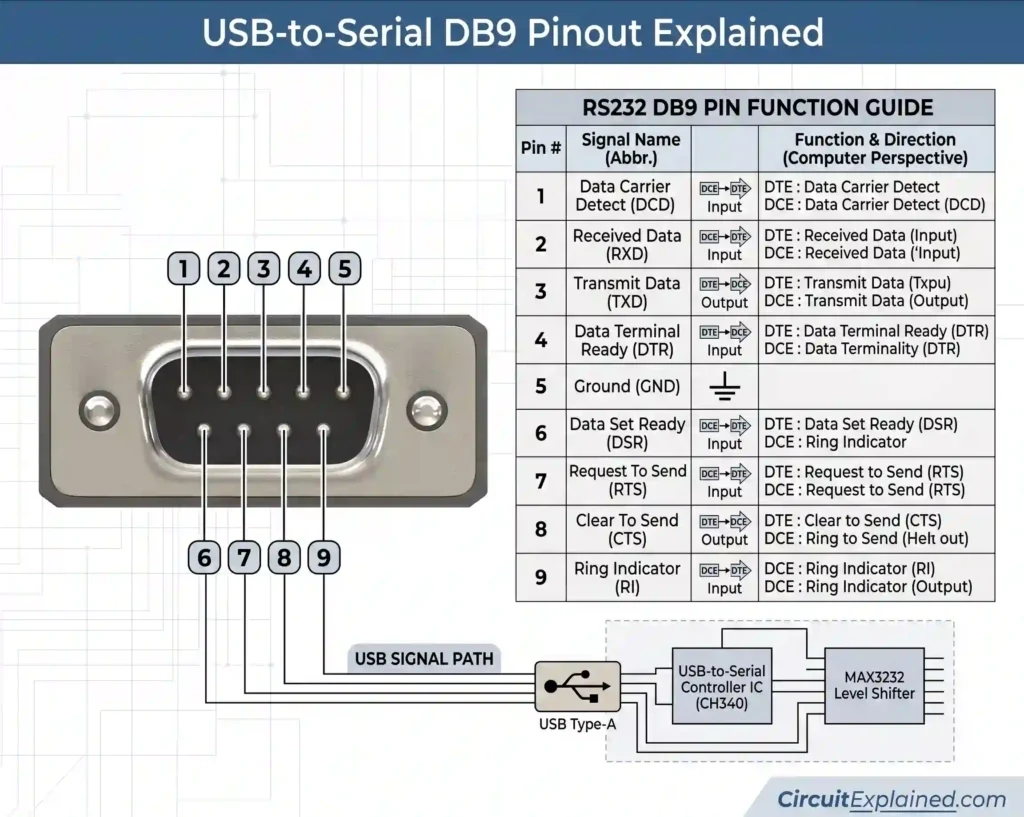
For quick reference when buzzing out your own legacy R232 cable or mapping the output of a new USB serial adapter, here is the standard DB9 pinout mapped to typical converter logic:
| Pin | Name | Direction (from PC) | Description |
| 1 | DCD | Input | Data Carrier Detect |
| 2 | RXD | Input | Receive Data |
| 3 | TXD | Output | Transmit Data |
| 4 | DTR | Output | Data Terminal Ready |
| 5 | GND | Common | Signal Ground |
| 6 | DSR | Input | Data Set Ready |
| 7 | RTS | Output | Request to Send |
| 8 | CTS | Input | Clear to Send |
| 9 | RI | Input | Ring Indicator |
What’s Inside the Adapter?
Getting inside one of these adapters usually involves carefully slicing through the overmolded rubber casing or prying apart a sonic-welded plastic shell. Once you strip away the exterior, you are left with a surprisingly dense little printed circuit board (PCB) crammed right behind the DB9 connector.
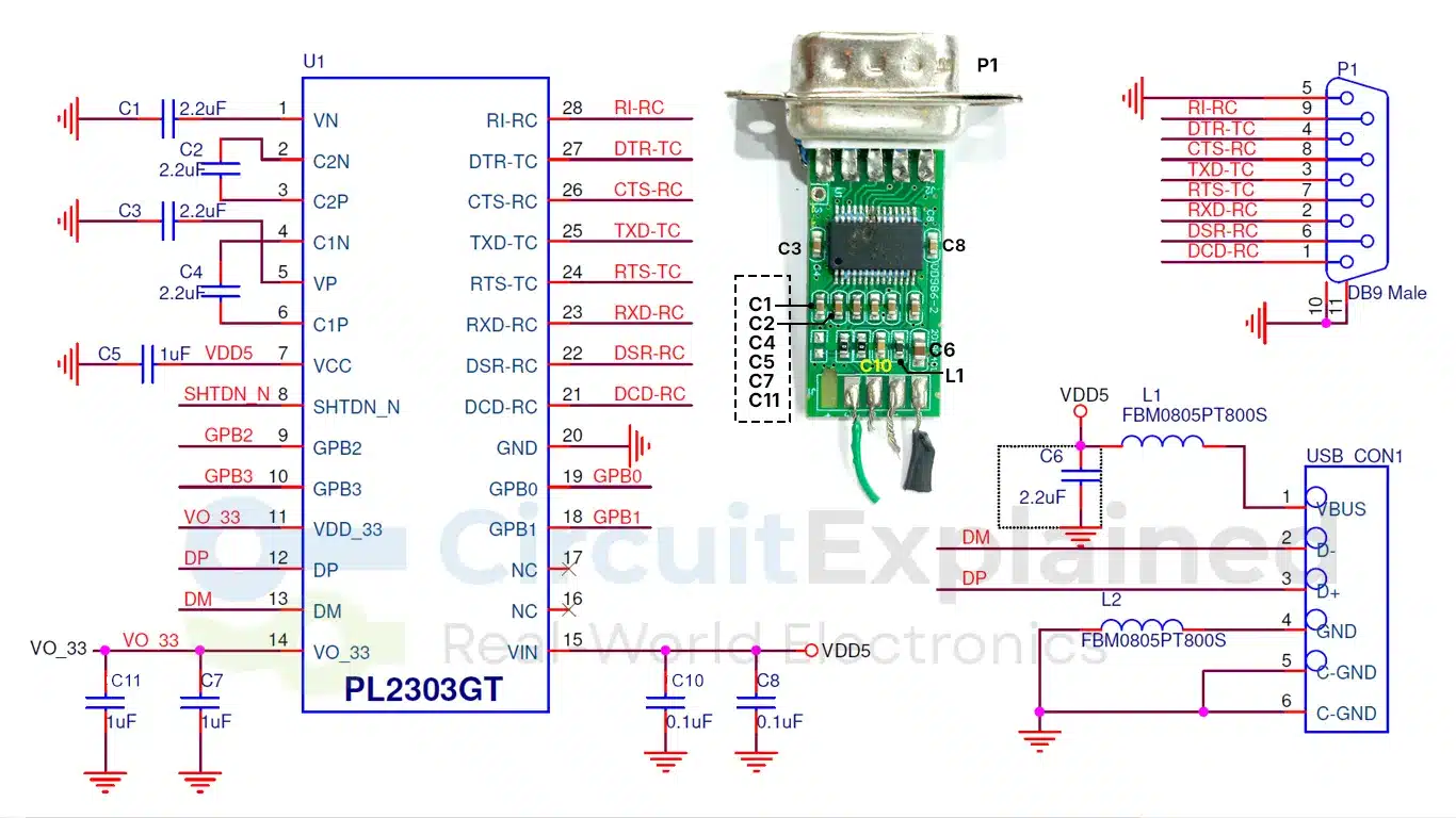
While cutting away the overmolded housing, the mechanical stress caused the shield wire’s connector pad to delaminate from the circuit board. This lifted trace is clearly visible in the teardown photos.
If you were opening up an older or cheaper adapter, you would typically expect to find two distinct integrated circuits (ICs) taking up most of the board space: one chip to translate the USB signals, and a second chip to boost the voltage.
However, looking closely at this specific PCB reveals a much more elegant, modern engineering solution.
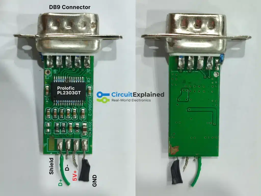
Instead of a cluttered dual-chip layout, this board is dominated by a single, all-in-one powerhouse: the Prolific PL2303GT.
This single IC acts as a complete bridge between the USB port and the serial peripheral, tackling two entirely different engineering challenges simultaneously:
- 1. The USB to UART Bridge: First, the PL2303GT handles the complex digital translation. USB communicates using fast, differential data packets. The front-end of this chip takes those raw USB packets and converts them into a standard, logic-level UART (Universal Asynchronous Receiver-Transmitter) serial stream.
- 2. The Integrated RS232 Transceiver: Standard 5V logic is fragile over long distances and completely incompatible with true RS232 hardware. In older designs, a secondary chip (like a MAX232) was required to boost the voltage. The PL2303GT, however, has a high-voltage RS232 transceiver baked right into the silicon. It takes its own internal logic signals and aggressively bumps them up to the rugged, high-voltage levels required by the RS232 standard (typically around ±7V to ±15V).
While the PL2303GT handles the heavy lifting, you will still notice a cluster of tiny passive components mostly surface-mount capacitors surrounding the chip.
This brings up a fascinating engineering question: how does a single IC output a -12V or +12V RS232 signal when the USB port it is plugged into only provides a flat 5V?
The answer lies in those capacitors and the internal charge pump, which is exactly what we are going to trace out in the schematic next.
Schematic Analysis: Tracing the PL2303GT
When you look at the schematic for this adapter, the beauty lies in its simplicity. Because the PL2303GT is a highly integrated System-on-Chip (SoC), it absorbs almost all of the complexity that used to require a board full of discrete components.
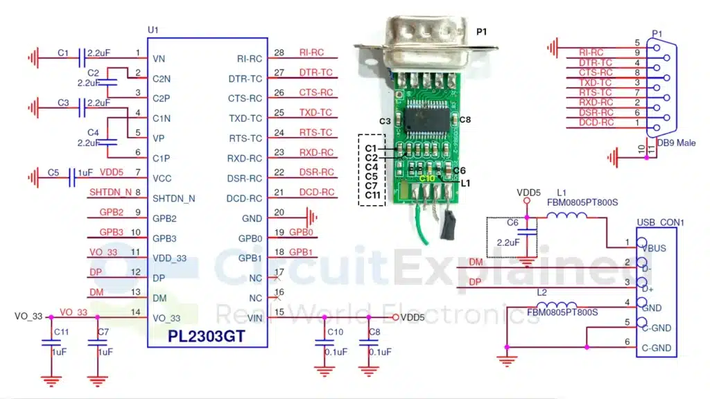
Starting from the USB Type-A connector, the 5V (V_BUS) and Ground lines feed directly into the IC to power the internal logic. The USB differential data lines (D+ and D-) are routed straight into the chip’s USB transceiver pins. Older USB-to-Serial designs required an external crystal oscillator to maintain precise USB timing, but the PL2303GT features a built-in precise clock generator, completely eliminating the need for an external crystal and freeing up valuable PCB real estate.
When examining the mechanical layout alongside the schematic, shielding is critical. To ensure noise immunity in harsh industrial environments, the earth ground and chassis ground should be consolidated into a single screw hardware mechanism on the board. This solidly ties the USB shield and the DB9 metal housing together, protecting the delicate data lines from electromagnetic interference (EMI) without creating fragile or messy ground loops.
The Magic of the Charge Pump
The most fascinating part of this schematic isn’t the data routing; it is the power delivery. The RS232 standard requires voltage swings far outside the standard 5V provided by a USB port. A logic “LOW” (space) sits between +3V and +15V, while a logic “HIGH” (mark) sits between -3V and -15V.
So, how does the PL2303GT generate negative voltages and double-digit positive voltages from a flat 5V USB supply? It uses an internal charge pump.
If you look closely at the schematic around the PL2303GT, you will see a cluster of external capacitors (typically 0.1uF or 1uF) connected to specific pins (often labeled V+, V-, C1+, C1-, etc.). These passive components are the lungs of the charge pump. Here is how the IC uses them:
- Voltage Doubling: The IC contains internal electronic switches that rapidly alternate. During the first phase, it connects one of the external capacitors across the 5V USB supply, charging it up. In the next split-second phase, it flips the switches to place that fully charged capacitor in series with the 5V supply. Like stacking two 5V batteries end-to-end, this instantly boosts the internal voltage to nearly +10V.
- Voltage Inverting: To get the required negative voltage, the chip uses another set of switches and a second capacitor. It takes the newly generated +10V, charges the second capacitor, and then flips its connection entirely backward relative to ground. This clever switching effectively pulls the output below ground, generating approximately -10V.
By rapidly switching these tiny external capacitors thousands of times per second, the PL2303GT continuously pumps out the high bipolar voltages (10V to 12V) needed to drive signals down a long, noisy industrial serial cable. The remaining pins on the DB9 connector simply route these high-voltage signals directly out of the IC’s integrated transceiver to your legacy hardware.
Common Issues & Driver Headaches
If you work with serial adapters long enough, you are guaranteed to run into one of two major headaches: mysterious driver failures or fried hardware. Here is what you need to know to avoid both.
1. Counterfeit Chips and “Bricked” Drivers
The market is absolutely flooded with cloned USB-to-serial chips. Because genuine FTDI and Prolific ICs are the industry standard, overseas manufacturers have spent years producing unauthorized silicon clones that mimic the original chips.
For a while, these clones worked perfectly. However, the original manufacturers eventually fought back through Windows driver updates. In infamous industry events, official driver updates were pushed out that could detect counterfeit silicon. If a fake chip were detected, the driver would intentionally refuse to work, sometimes throwing a frustrating “Code 10: This device cannot start” error or, worse, silently rewriting the clone chip’s internal ID to effectively “brick” the cable permanently.
The Fix: If you are buying an adapter for critical industrial gear, do not buy the cheapest generic cable available online. Look for reputable brands (like the Z-TEK cable we tore down) that guarantee genuine silicon, or ensure you are specifically buying a cable with a newer generation chip like the PL2303GT or CH340, which currently have fewer counterfeit driver issues.
For the PL2303GT, you can download drivers from its official Prolific website below.
https://www.prolific.com.tw/en/portfolio-item/pl2303gt/
PL2303GT Reference Schematic Design (Built-in RS232 Transceiver).
Download Reference Circuit Diagram PDF2. The Voltage Level Trap: RS232 vs. TTL
This is the number one way beginners destroy their microcontrollers.
Because we call these “USB to Serial” adapters, it is easy to assume you can connect them to any device that uses serial communication. Do not plug this cable directly into an Arduino, ESP32, or Raspberry Pi.
- Microcontroller Serial (TTL/CMOS Logic): An ESP32 or Arduino communicates using 3.3V or 5V logic. A logic “HIGH” is 3.3V, and a logic “LOW” is 0V.
- True RS232 Serial: As we saw in our charge pump analysis, true RS232 pushes signals at ±12V.
If you connect the RX/TX pins of a standard DB9 RS232 cable to the RX/TX pins of your 3.3V microcontroller, that ±12V spike will instantly destroy the MCU’s input pins and likely let the magic smoke out of the entire board.
The Fix: If you want to talk to a raw microcontroller, you do not want an RS232 adapter; you need a USB-to-TTL adapter (which is essentially the first half of our teardown circuit, completely omitting the voltage-boosting charge pump). If you must use an RS232 cable, you need to put a separate MAX3232 transceiver circuit in between the cable and the MCU to safely step those high voltages back down to 3.3V.
Conclusion
It is easy to take a simple cable for granted, but as this teardown shows, there is some serious engineering happening inside that molded DB9 housing. We traced the journey of a delicate, high-speed USB differential pair as it entered the silicon of the PL2303GT.
Whether you are using a premium Z-TEK adapter or a generic clone, this invisible, real-time conversion is the only reason our modern laptops can still communicate with the backbone of our industrial and networking infrastructure.
Let me know what you are hooking your adapter up to in the comments below!